
Dans le domaine de la microfabrication moderne, peu de matériaux sont aussi largement utilisés que le SU-8 pour créer des structures à micro-échelle destinées à des dispositifs tels que les systèmes de type « laboratoire sur unepuce » et les biocapteurs. Le SU-8 joue un rôle central dans la les processus de lithographie souple , en particulier dans la fabrication de moules maîtres utilisés pour reproduire des canaux microfluidiques et d’autres éléments à l’échelle nanométrique ou microscopique avec une grande fidélité de motif dans des matériaux tels que le le PDMS.
Sa capacité à produire des structures précises, durables et présentant un rapport d'aspect élevé a fait du SU-8 un « résine photosensible » de choix pour un large éventail d'applications de microfabrication.
Cet article examine les propriétés, les procédés de fabrication et les applications du SU-8 résine photosensible, en mettant particulièrement l'accent sur son utilisation dans les fabrication de dispositifs microfluidiques et la production de moules maîtres pour la lithographie douce.
Qu'est-ce que le SU-8 résine photosensible?
Le SU-8 est une résine photosensible e négative à base d’époxy e largement utilisée en photolithographie pour créer des structures microscopiques épaisses et très résistantes. Le terme « négatif » fait référence à son comportement lors de l’exposition aux UV : les zones exposées à la lumière se solidifient et se réticulent chimiquement, tandis que les zones non exposées restent solubles et peuvent être éliminées par lavage lors du développement. Le chiffre 8 dans SU-8 correspond au nombre moyen de groupes époxy s présents dans sa structure moléculaire, qui contribuent à la réticulation importante conférant au matériau sa résistance et sa stabilité après traitement.
Le SU-8 est disponible sous plusieurs formulations époxy résine permettant la fabrication de structures présentant différentes épaisseurs et différents rapports d'aspect. Cette polyvalence a contribué à son adoption généralisée dans les environnements de prototypage.
Pourquoi le SU-8 est-il si largement utilisé dans la microfabrication ?
Le SU-8 est largement utilisé dans la microfabrication car il permet de fabriquer des microstructures épaisses à rapport d'aspect élevé, avec une excellente précision dimensionnelle et une grande fidélité de reproduction des motifs. Il est entièrement compatible avec les procédés de photolithographie standard et est disponible en plusieurs formulations pour s'adapter à une large gamme d'épaisseurs de film.
Une fois durci, le SU-8 offre une résistance mécanique élevée, une résistance chimiqueet une stabilité à long terme, ce qui en fait l’ résine photosensible e de choix pour des applications telles que les moules maîtres microfluidiques, les MEMS, les biocapteurs, la micro-optique et les dispositifs de type « laboratoire sur unepuce ».
Le rôle du SU-8 dans la lithographie douce
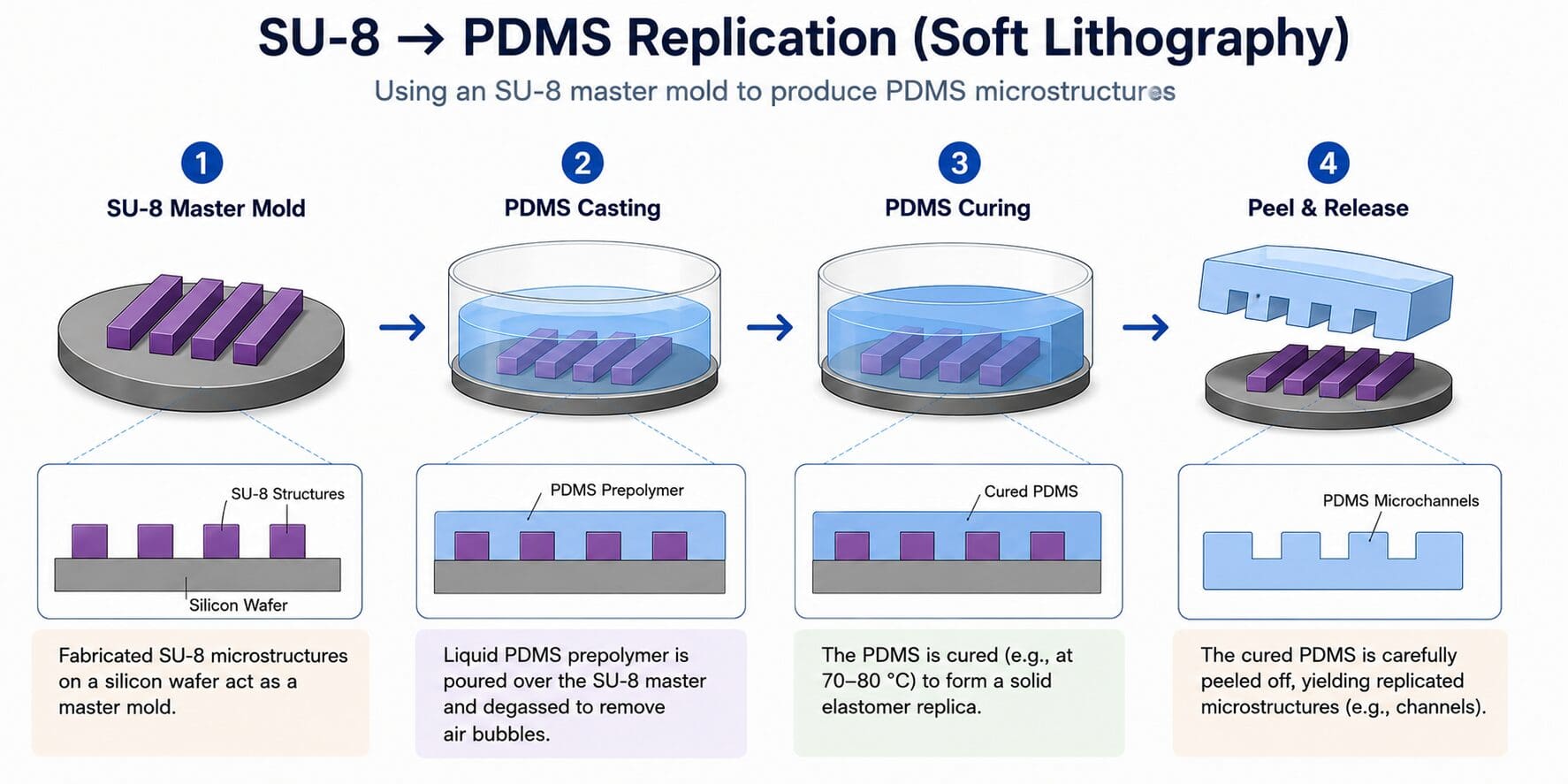
En lithographie douce, le SU-8 est principalement utilisé pour fabriquer le moule maître à partir duquel les dispositifs microfluidiques sont reproduits. Sa capacité à produire des microstructures précises, à rapport d'aspect élevé et dotées d'une excellente stabilité dimensionnelle en fait un matériau de moulage idéal pour le moulage du PDMS. Un seul moule maître en SU-8 pouvant être réutilisé plusieurs fois, il permet un prototypage rapide, une reproductibilité élevée et une fabrication rentable de dispositifs microfluidiques.
Lithographie SU-8 : le procédé clé
La fabrication des microstructures en SU-8 suit un processus de photolithographie standard, dans lequel chaque étape de traitement influe sur la précision, la qualité et la reproductibilité finales des microstructures obtenues.
Bien que les paramètres du procédé varient en fonction de la taille souhaitée des structures et de l'épaisseur de la résine photosensible, la séquence globale reste globalement la même : préparation de la plaquette, enduction par centrifugation, cuisson douce, exposition aux UV à travers un photomasque, cuisson post-exposition, développement et, si nécessaire, une cuisson finale à haute température afin d'améliorer encore la stabilité mécanique et chimique des structures en SU-8.
Les sections suivantes décrivent l'objectif et les points clés à prendre en compte pour chaque étape.
Préparation des plaquettes
Une préparation adéquate de la plaquette permet d'obtenir une surface propre et stable, garantissant un dépôt uniforme du SU-8, et améliore la qualité et la reproductibilité des microstructures finales.
Par conséquent, avant l'application du SU-8, le substrat — généralement une plaquette de silicium— doit être soigneusement nettoyé afin d’éliminer les particules, les résidus organiques et l’humidité susceptibles d’affecter l’ résine photosensible l’adhérence et l’uniformité du revêtement. Dans de nombreux processus de fabrication, la plaquette est également déshydratée par chauffage afin d’améliorer l’adhérence et de minimiser les défauts lors des étapes de photolithographie suivantes.
Revêtement par centrifugation : création d'un film uniforme
Le revêtement par centrifugation est la première étape de traitement après la préparation du substrat et la méthode la plus couramment utilisée pour déposer du SU-8 sur une plaquette de silicium. Au cours de cette étape, du SU-8 liquide est déposé au centre du substrat, qui est ensuite mis en rotation à grande vitesse (généralement plusieurs milliers de tr/min) afin d'étaler l'résine photosensible e en un film mince et uniforme sous l'effet de la force centrifuge.
L'épaisseur finale du film dépend principalement de la vitesse de rotation, de la viscosité de la résine photosensible et des paramètres de dépôt. Il est essentiel d'obtenir un dépôt uniforme, car les variations d'épaisseur, les microbulles ou les impuretés de surface peuvent nuire aux étapes suivantes de cuisson, d'exposition aux UV et à la qualité du motif.
💡 Astuce pour le revêtement par centrifugation : après avoir déposé le SU-8 sur la plaquette, laissez reposer quelques minutes avant de lancer la centrifugation. Cela permet aux microbulles piégées de remonter à la surface et d'éclater, ce qui améliore l'uniformité du revêtement.
Cuisson douce : élimination du solvant et stabilisation du film
Après l'enduction par centrifugation, la couche de SU-8 contient encore des résidus de solvant (généralement entre 5 et 20 %) qui doivent être éliminés avant l'exposition aux UV. Le « soft bake » permet d'éliminer ce solvant, de stabiliser l'résine photosensible, d'améliorer l'adhérence et de préparer le film en vue d'un transfert précis du motif.
Cette étape se déroule généralement en deux phases thermiques : une première cuisson à basse température (environ 65 °C) pour évaporer progressivement le solvant, suivie d'une cuisson à température plus élevée (environ 95 °C) dont la durée dépend de l'épaisseur de la résine photosensible, afin de consolider davantage le film. La plaquette doit ensuite refroidir progressivement jusqu'à température ambiante.
Un chauffage trop rapide peut piéger le solvant sous une couche superficielle durcie, créant ainsi des contraintes internes susceptibles d'entraîner une mauvaise qualité du motif ou l'apparition de fissures. À l'inverse, un séchage insuffisant entraîne souvent une élimination incomplète du solvant, ce qui peut nuire à l'exposition aux UV et au développement ultérieurs.
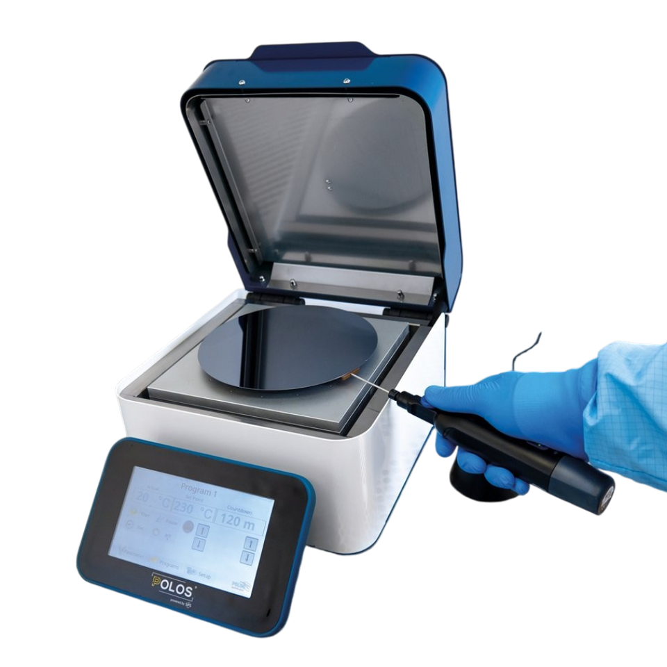
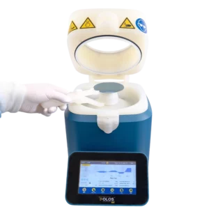
💡 Astuce de cuisson douce : utilisez une programmable plaque chauffante dans la mesure du possible plutôt qu’un four à convection. Elle assure une distribution de la température plus homogène, ce qui permet une meilleure élimination du solvant et réduit les contraintes, en particulier dans les couches épaisses de SU-8.
Exposition aux UV et structuration des masques
Une fois la cuisson douce terminée, la couche de SU-8 est alignée avec un photomasque comportant le motif souhaité, puis exposée à une lumière UV proche (généralement autour de 365 nm).
Selon l'application, on peut utiliser soit des photomasques positifs (motifs transparents sur fond opaque), soit des photomasques négatifs (motifs opaques sur fond transparent). Pour les dispositifs microfluidiques, cependant, ce sont les photomasques négatifs qui sont les plus courants, car ils permettent de conserver les structures d'canal s souhaitées après le développement.
Lors de l'exposition, les zones transparentes du photomasque laissent passer la lumière UV, qui active le SU-8 exposé, déclenchant ainsi les réactions chimiques qui donneront naissance ultérieurement aux microstructures réticulées (lors de la cuisson post-exposition).
💡 Conseil concernant l'exposition aux UV : la géométrie et la qualité des structures finales dépendent en grande partie de la précision de l'alignement du masque et d'une dose d'exposition adéquate. Une exposition excessive aux UV peut réduire la résolution des structures et déformer les parois latérales, tandis qu'une exposition insuffisante peut entraîner une réticulation incomplète et une mauvaise définition du motif.
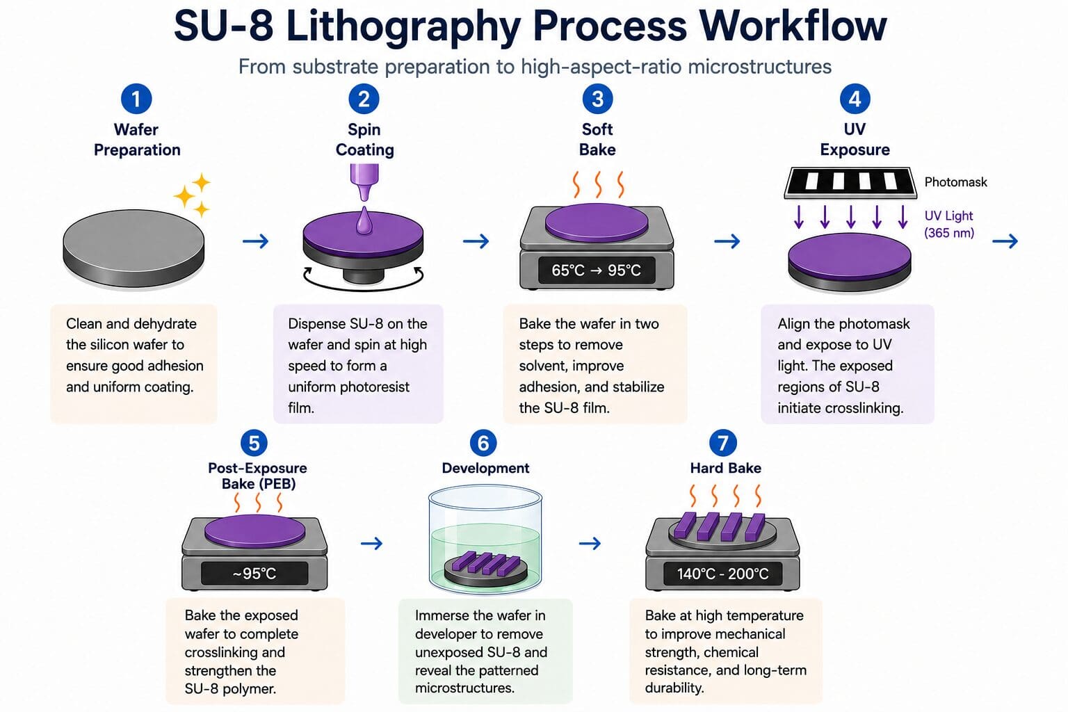
Cuisson post-exposition (PEB) : achèvement de la réticulation
À l'issue de l'étape de lithographie UV, la plaquette subit un traitement thermique post-exposition (PEB), qui achève les réactions de réticulation amorcées pendant l'exposition. À l'instar du traitement thermique doux, la plaquette est chauffée progressivement jusqu'à environ 95 °C, ce qui active l'acide photogénéré et permet aux groupes d'époxy s présents dans le SU-8 de se polymériser complètement pour former une structure polymère mécaniquement résistante et chimiquement stable.
Étant donné que le degré de réticulation influe directement sur la fidélité du motif et l'intégrité structurelle, le PEB constitue l'une des étapes les plus critiques du processus de fabrication du SU-8.
💡 Conseil pour la cuisson post-exposition : utilisez un profil de chauffage et de refroidissement lent et contrôlé pendant la cuisson post-exposition (PEB), en particulier pour les couches épaisses de SU-8. Les variations rapides de température peuvent générer des contraintes internes, entraînant une déformation du motif ou l'apparition de fissures.
Développement : dévoilement de la structure finale
Au cours du développement, la plaquette est immergée dans une solution de développement (généralement du PGMEA ou un révélateur SU-8 spécifique) qui dissout les parties non exposées et non réticulées de l'résine photosensible, révélant ainsi les microstructures SU-8 définitives.
On recourt souvent à une agitation douce pour améliorer l'efficacité du développement. La durée du développement doit être soigneusement contrôlée afin de garantir l'élimination complète de l'résine photosensible e non exposée sans endommager les motifs.
💡 Conseil de développement : après le développement, rincez la plaquette avec du PGMEA frais ou de l'alcool isopropylique (IPA). Si un résidu blanc ou trouble apparaît lors du rinçage à l'IPA, cela signifie probablement que le SU-8 n'est pas suffisamment développé en raison de la présence de résine photosensible non réticulée. Remettez la plaquette dans le bain de développement pendant un certain temps, puis rincez-la à nouveau à l'IPA. Si la plaquette reste limpide lors du rinçage à l'IPA, le développement est probablement terminé.
Cuisson à haute température : renforcement du moule final
Une fois le développement terminé, il est possible de procéder à une cuisson à haute température (facultative) afin de renforcer davantage les structures en SU-8. Cette étape s’avère particulièrement utile lorsque le modèle en SU-8 est destiné à être utilisé à plusieurs reprises pour le moulage de PDMS et le collage ultérieur des composants.
Généralement réalisé à des températures comprises entre 140 °C et 200 °C pendant environ 20 à 30 minutes, ce traitement thermique supplémentaire améliore la dureté mécanique, la résistance chimique et la durabilité à long terme, tout en réduisant la quantité de solvant résiduel.
Difficultés courantes rencontrées lors de l'utilisation du SU-8
Malgré ses nombreux avantages, le traitement du SU-8 nécessite un contrôle rigoureux à chaque étape de la photolithographie. Parmi les difficultés les plus courantes, on peut citer :
- Mauvaise adhérence au support
- Formation de bulles d'air lors du revêtement par centrifugation
- Formation de la moulure de bordure
- Fissuration due à des contraintes thermiques internes
- Surexposition ou sous-exposition lors de la lithographie UV
- Développement incomplet
- Résidus de résine (dépôts)
- Déformation des motifs dans des couches épaisses de SU-8
La plupart de ces défauts peuvent être réduits au minimum grâce à une préparation adéquate du substrat, à des conditions de cuisson optimisées, à des doses d'exposition précises et à un développement contrôlé.
SU-8 contre Hare SQ™
Le SU-8 et HARE SQ™ sont des photorésines négatives à base d’ époxy, conçues pour la fabrication de microstructures à rapport d’aspect élevé. Ils partagent de nombreuses caractéristiques, notamment une excellente résistance mécanique, une bonne résistance chimique et une compatibilité avec les procédés standard de photolithographie UV. Ces deux matériaux sont largement utilisés pour les matrices de microfluidique, les MEMS, la micro-optique et d’autres applications à l’échelle microscopique.
Les principales différences résident dans leurs caractéristiques de mise en œuvre et les formulations disponibles. Le SU-8 est la référence du secteur depuis des décennies ; il offre une large gamme de viscosités, des protocoles de mise en œuvre bien établis et bénéficie d’une large adoption tant dans la recherche que dans la microfabrication industrielle. Le HARE SQ™ est une alternative plus récente qui s’intègre facilement aux processus de fabrication existants utilisant le SU-8, tout en offrant un prix compétitif, une transparence optique améliorée, une meilleure pureté et une plus grande homogénéité d’un lot à l’autre.
| Caractéristique | SU-8 | Hare SQ™ |
|---|---|---|
| résine photosensible type | Négatif époxy résine photosensible | Négatif époxy résine photosensible |
| Applications typiques | Microfluidique, MEMS, micro-optique | Microfluidique, MEMS, micro-optique |
| Structures à rapport d'aspect élevé | ✓ | ✓ |
| Capacité de traitement des couches épaisses | ✓ | ✓ |
| Résistance mécanique | Excellent | Excellent |
| Résistance chimique | Excellent | Excellent |
| Photolithographie UV standard | ✓ | ✓ |
| Fabrication de moules maîtres | ✓ | ✓ |
💡 Conclusion
Le SU-8 reste l’un des photorésines les plus utilisés en microfabrication en raison de sa polyvalence, de sa durabilité et de sa capacité à produire des structures à l’échelle microscopique de haute qualité. Associé à la photolithographie standard, il reste le matériau de prédilection pour la fabrication de matrices microfluidiques ainsi que d’une large gamme de dispositifs MEMS et de dispositifs de type « laboratoire sur une puce » (puce ).
Restez à l'écoute pour découvrir d'autres analyses sur les résines photosensibles SU-8, la lithographie souple, la microfabrication, la microfluidique sur PDMS et d'autres techniques stimulant l'innovation dans les dispositifs microfluidiques 🔬 !
📧 Si vous avez des questions ou des commentaires, n'hésitez pas à nous contacter à l'adresse contact@darwin-microfluidics.com.
❓ FAQ : SU-8 résine photosensible
Qu'est-ce que le SU-8 résine photosensible?
Le SU-8 est une résine photosensible à base d'époxy, un matériau photosensible utilisé en photolithographie pour créer des motifs microscopiques épais et à rapport d'aspect élevé sur un substrat, destinés à des applications de microfabrication.
Pourquoi le SU-8 est-il qualifié d'résine photosensible e négatif ?
Le SU-8 est qualifié d'résine photosensible e négatif car les zones exposées aux rayons UV se durcissent et restent fixées sur le substrat, tandis que les zones non exposées restent molles et sont éliminées par lavage lors du processus de développement.
À quoi sert le SU-8 ?
Le SU-8 est couramment utilisé pour la fabrication de moules maîtres microfluidiques, de dispositifs MEMS, de biocapteurs, de composants micro-optiques et de systèmes de type « laboratoire sur une puce » (puce ).
Pourquoi utilise-t-on couramment le SU-8 pour les moules maîtres microfluidiques ?
Le SU-8 est couramment utilisé pour la fabrication de moules maîtres microfluidiques, car il permet d'obtenir des structures durables et à haute résolution, dotées de parois verticales lisses, ce qui facilite la reproduction répétée et précise de dispositifs microfluidiques en PDMS.
Quelles sont les principales étapes du procédé de photolithographie SU-8 ?
Un procédé SU-8 type comprend la préparation du substrat, le revêtement par centrifugation, une cuisson préliminaire, une exposition aux UV à travers un photomasque, une cuisson post-exposition, le développement et, éventuellement, une cuisson finale.
Pourquoi la cuisson post-exposition (PEB) est-elle importante pour le SU-8 ?
La cuisson post-exposition achève les réactions de réticulation amorcées lors de l'exposition aux UV, conférant ainsi au SU-8 structuré sa résistance mécanique, sa résistance chimique et sa stabilité dimensionnelle.
Quels sont les principaux défis rencontrés lors du traitement du SU-8 ?
Parmi les problèmes courants, on peut citer une mauvaise adhérence, la présence de bulles d'air, des fissures dues aux contraintes thermiques, une surexposition ou une sous-exposition, un développement incomplet et la présence de résine photosensible résiduelle après le développement.
Pourquoi des fissures apparaissent-elles dans le SU-8 au cours du processus de fabrication ?
Les fissures sont généralement dues à des contraintes internes excessives résultant d'un échauffement ou d'un refroidissement rapide, de conditions de cuisson inadaptées ou de couches épaisses de SU-8 sur des substrats présentant des propriétés de dilatation thermique différentes.
Pourquoi des bulles d'air se forment-elles lors du revêtement par centrifugation du SU-8 ?
Des bulles d'air peuvent se former lors du revêtement par centrifugation en raison d'une application incorrecte de la résine photosensible ou de la présence d'air emprisonné. Laisser reposer brièvement le SU-8 avant la centrifugation permet aux bulles de remonter à la surface et de disparaître.

🔗 Références
- Mata, A., Fleischman, A. J. et Roy, S. (2006). Fabrication de microstructures multicouches en SU-8. Journal of micromechanics and microengineering, 16(2), 276-284. https://doi.org/10.1088/0960-1317/16/2/012
- Yang, R., & Wang, W. (2006). Lithographie UV de SU-8 ultra-épais pour la microfabrication de microstructures à rapport d'aspect élevé et applications dans les composants microfluidiques et optiques. Bio-MEMS : Technologies et applications, 11.
- Keller, S., Blagoi, G., Lillemose, M., Haefliger, D. et Boisen, A. (2008). Traitement de films minces de SU-8. Journal of micromechanics and microengineering, 18(12), 125020. https://doi.org/10.1088/0960-1317/18/12/125020
- Martinez-Duarte, R., & Madou, M. (2011). La photolithographie SU-8 et son impact sur la microfluidique. Manuel de microfluidique et de nanofluidique, 38.
- Lee, J. B., Choi, K.-H. et Yoo, K. (2015). Techniques innovantes de lithographie SU-8 et leurs applications. Micromachines, 6(1), p. 1-18. https://doi.org/10.3390/mi6010001